Part 10 : "Nikon FE"
An AE version of the Nikon FM

The arrival of the Nikon FE (see photograph) was an eagerly awaited event.
Following the Nikon FM launched in 1977 (Part 9. of this series), it seemed to be the natural progression, with the same compact body as the FM, electronically controlled shutter and aperture priority AE.
In fact, the development of the FE started long before the commercial launch of the Nikon FM and the Nikon EL2. As already mentioned in "Nikon EL2" (Part 8. of this series), it was the fact that the planning of the Nikon FE was already underway that investigated the clever idea of providing a wide power supply voltage, so that the same control microchips could be used.
I, the author, was also a member of the FE development team, and I felt somewhat strange that the previous model, the EL2, was still not yet on the market when the FE development was in full swing.
Trying new ideas
The Nikon FE (See photo) went on sale in June 1978, about one year after Nikon had switched to the AI (Automatic Maximum Aperture Indexing) system. The apparent specification is orthodox, and unpretentious, but this gave it, together with the Nikon FE2, a long-term popularity with many fans. Inside, this camera incorporates a number of experimental new ideas from Nippon Kogaku which make it an adventurous product.
The phantom "boomerang"
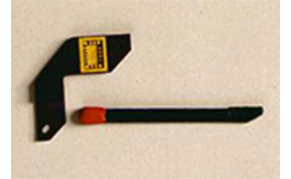
and a match
One product of the design experiments did not make it to manufacture.
For many years, an experimental component for the FE, the size of a match head, has been lying in a drawer of my desk.
This component was an integrated circuit package intended for the FE, and known because of its shape as the "boomerang."
To describe the circumstances behind this, I had better start by talking about the photo sensors used for light metering.
Nippon Kogaku adopted a SPD (silicon photodiode) as the photodetector for the EL2 and the F2 Photomic SB, and a GPD (gallium arsenide phosphide photodiode) for the FM.
Compared with the CdS elements previously used, these have a much faster response, and good characteristics, but the output current is much smaller.
A slight imperfection in the circuit insulation, and the current can leak away, preventing accurate light metering.
Very special care had to be taken, therefore, in assembling the circuit to make sure that the connection between the photo sensor and the control chip's input terminals was properly insulated and protected from influence of external noise.
To prevent leakage currents and protect from influence of noise, we wanted to make the connection from the photo sensor to the control chip as short as possible, and seal it within the circuit board. "Well," we thought, "In that case why not put the photo sensor inside the control chip package ?"
Meanwhile, there had always been two (2) photo sensors, one on each side of the viewfinder eyepiece, but we had a plan to replace these by one element above the eyepiece.
The integrated circuit package mentioned above was an experimental result of this plan.
The boomerang-shaped package was arranged on the eyepiece side of the viewfinder pentaprism, extending to the side from over the eyepiece lens.
The leads from the photo sensor entered two (2) holes arranged vertically on the top of the package, and were soldered.
The integrated circuit chip was enclosed in the hollow underneath, with a metal covering seal.
The package had a multilayer construction, with internal interconnects between the photodetector and integrated circuit chip, and then the terminals of the chip were connected from the back of the package to the flexible printed circuit (FPC).
If implemented this would have been a revolutionary design.
Ambushed !
Unfortunately, an unexpected trap brought this plan to an abrupt halt. For various other reasons the plan to have a single photo sensor on the eyepiece was abandoned, and the design suddenly reverted to the original arrangement with two sensors. So the "boomerang plan" was dropped.
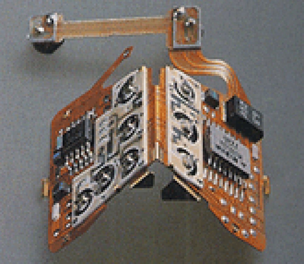
Now the two (2) photo sensors were soldered to extensions of the flexible printed circuit extending over the eyepiece lens, and the signals taken to a chip mounted on the pentaprism. Of course, great care was taken to prevent current leakage, and the interconnects were shielded by a protective covering.
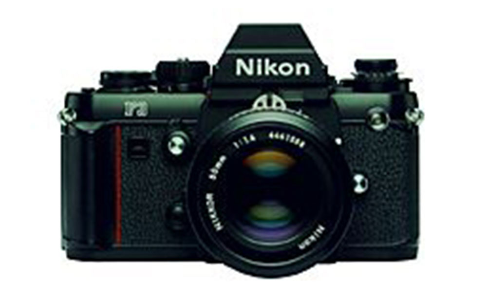
The boomerang plan was abandoned, but the idea of attaching a photo sensor directly to the integrated circuit package was carried forward with great success to the Nikon F3 (See photo), which went on sale in 1980.
The SPD photodetector element in the bottom of the body is directly attached to the integrated circuit package which includes the light metering circuit.
With the latest advances, the SPD photodetector chip now usually includes a preamplifier for light metering.
Remove the leads from the electronic components !
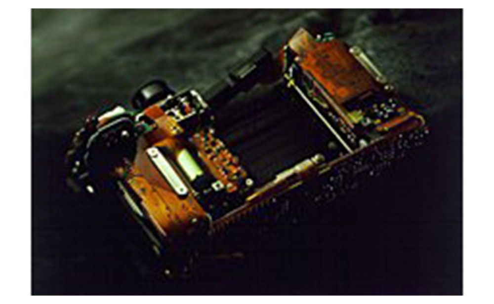
The FE was an adventurous model in terms of its electric mounting. It introduced the electronic shutter to the single-lens reflex design, and with TTL-AE the electronic parts suddenly took up a much larger part of the camera. But it was not necessary to redesign the interior of the camera body to accommodate the electronics, which were fitted skillfully into gaps which had previously only been wasted space.
An important role in this was played by the flexible printed circuit (FPC), which serves as both circuit board and wiring.
With experience gained from the EL2, Nippon Kogaku was now skilled in the use of flexible printed circuits. But the conventional design, with capacitors, resistors, and other components soldered to the flexible substrate by their leads, made it difficult to make the printed circuit thinner.
The strategy adopted was to eliminate all leads from the components, and replace them with chip components.
When a number of variable resistors were needed for light metering and similar adjustments, a resistor block on a ceramic substrate was used, and the technology for a direct, leadless mounting on the flexible printed circuit had already been developed for the EL2.
With a switch to tantalum capacitors and fixed resistors in chip component form, the technology was developed to mount all of these components on the flexible printed circuit by a single operation of reflow soldering. This was a foretaste of the surface mounting technology for miniature electronic components which is used even now.
Thereafter, the shift to electronics in cameras continued, with the flexible printed circuit getting larger and larger.
The number of electronic components is now vastly greater than then, but the foundations of the technology were laid down with the FE.
"Simple Nikon"
This catchphrase was used when the FE first went on sale in Japan (Nippon).
On the surface, this was a camera with basic specification, not appearing to be the most advanced model of its time, but actually it incorporated a number of exciting new ideas. In this sense, it was perhaps the starting point for the modern electronically controlled Nikon SLR.
Note
This issue first appeared in "Nikkor Club Quarterly" magazine , published by the Nikkor Club, and was revised for Nikon's webpage.
Products, brands and companies names are trademarks or registered trademarks of their respective companies.
Camera Chronicle
Archives of corporate history subject matter related to Nikon cameras, including rare materials, as well as product photos of cameras and lenses.